BillP's 256MB Infineon Module
For best viewing, your screen resolution should be 1024 x 768 or larger.
BiilP provided me with an Infineon 256MB PC100 CL2 SODIMM memory module (part number HYS64V32220GBDL-8-C2) since
there was some question whether or not it has 8 or 16 parts on it.
In other words, is it a "low-density" or "high-density" module? It has heat shields/spreaders on both sides of the
module so it is next to impossible to determine how many individual memory components are on the board without
bending back or breaking the covers. By looking through the contact edge of the module (where the gold "fingers"
are), there appears to be four distinct sections on each side, suggesting eight parts in total. It is not possible
to look through the "ends" of the module since the heat shield is bent down to the board, thus there is no way to
visually determine if there are 4 or 8 per side. According to what I found online for
an Infineon part numbering system (page 20), I initially thought that it was using 32M (addressing) devices,
which is normally "high" density. Looking at the document a little closer, I see that it says that the "component
organization" is 16M x 16. That means the addressing is in line with a "low density" module, it's just that it
uses 16-bit wide parts instead of 8-bit wide parts. If true, then there ARE only 8 parts on the module (eight 16M
x 16 parts = 256MB). This would be the exception to the rule that a 256MB module that has eight individual memory
chips is a high density version.
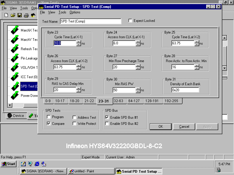
The screenshots on this page were taken from a Darkhorse Sigma-3 memory tester running under Windows 95. It shows
some selected operating screens; namely the module Identification Wizard and the Serial Presence Detect (SPD)
information from the Infineon module and a 512MB PC133 module as a comparison. The Sigma-3 tester has nine pages
of SPD information, arranged as tabs ("0-9", "10-17", "18-20", etc.). Each tab shows the contents of the selected
SPD bytes. The tester essentially "reads" the contents of the SPD bytes out of the EEPROM and displays them in these
pages for the engineer to examine and/or modify. Contained within the SPD bytes is information which can reveal
many things about the module. One of those is the refresh timing condition and therefore can say if it is a low or
high density compatible module. And as long as we are looking at some of these SPD bytes, I'll point out a couple
of other things along the way.
 |
| This first screenshot shows the result of the Darkhorse ID Wizard. This tester can identify what type of module
has been inserted into the test socket by running some tests to see how many address signals and output pins are
valid. In this case it has found a total of 256MB of memory (we knew that!) and that there are two banks of memory:
"(8) 4Mx8x4B" for both Banks 0 and 1. I believe this indicates that there are 8 parts per size ("(8)"), with each
device being organized as a 4M address range (the "4M" or 4*1024*1024), 4 internal banks ("4B") and 8 output pins.
Doing all of the math, that makes it 4,194,304 addresses times 4 internal banks times 8 output pins times 8 devices
times 2 sides, or 2,147,483,648 BITS of memory. To convert that to BYTES, divide by 8 and you get 268,435,456 or
what is normally called 256MB (256 * 1024 *1024). Note: Internal memory banks are really just extra
address pins. They do not have anything to do with how many parts are actually mounted on the module. However, this is
in opposition to what the Infineon document states; the module is supposed to be using 16 output pin devices. |
 |
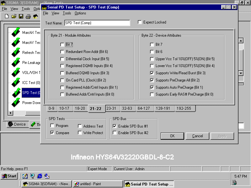
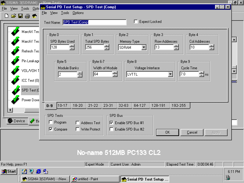
This is the first SPD screen showing a couple of important points: Bytes 3 and 4 are the total number of address
signals used. Taken together, this indicates that there are 22 address pins or a total of 4,194,304 memory addresses.
Combined with Byte 5 (number of module banks or physical sides; 2) and Byte 6 (number of data pins; 64), it almost
describes the total memory. What's missing is on the next page of SPD information. But before we get to that, there's
one more byte that is worth noting. Byte 9 (Cycle Time) indicates the clock speed of the module. 10ns = 100Mhz, or
PC100. |
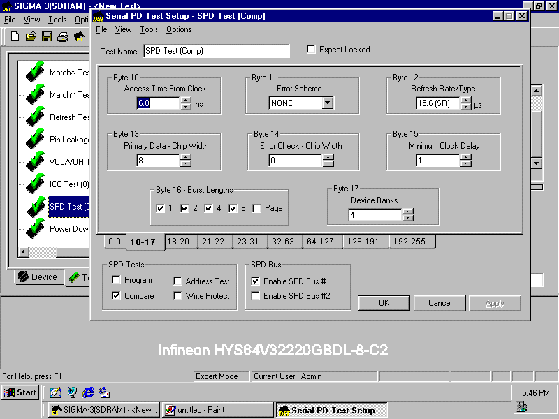 |
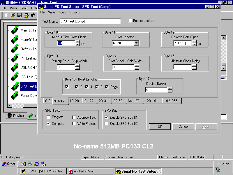
The second SPD screen shows two things of importance: Byte 17, which is the number of banks within each memory chip
and Byte 12, the Refresh Rate. As previously mentioned, the number of banks in each device can really be thought of
as additional addresses. So you would basically multiply the information in the first SPD page by 4 to come up with
the total number of bits in the module. The Refresh Rate parameter is particularly important since it is the main
difference between "low density" and "high density" memory. The way this value works is that it is the time interval
(in microseconds, or µs) between each refresh signal given to the memory array. DRAM requires that this signal
be sent to the memory every so often so that the data remains stored correctly. In this case, the Infineon module
says it requires a refresh pulse every 15.6µs. Each pulse refreshes some of the data that is stored in memory
(in actuality, a row or groups of rows). DRAM needs every row in the array refreshed within a certain amount
of time to guarantee that all data remains intact. The standard amount of time in which every row needs to "see"
this refresh interval is 64 milliseconds (ms; 1000µs = 1ms). If you take the refresh interval and divide it
by the Refresh Rate you arrive at the total number of cycles that is generated. So, 64ms / 15.6µs = 4,102.56.
Really, the number of cycles needed within the 64ms is 4,096 (2 to the power of 12); there is a rounding error in
the Refresh Rate box since the real value is 15.625µus. In any event, this is what is normally referred to as
"4K refresh" and is the deciding factor of a memory being "low density".
|
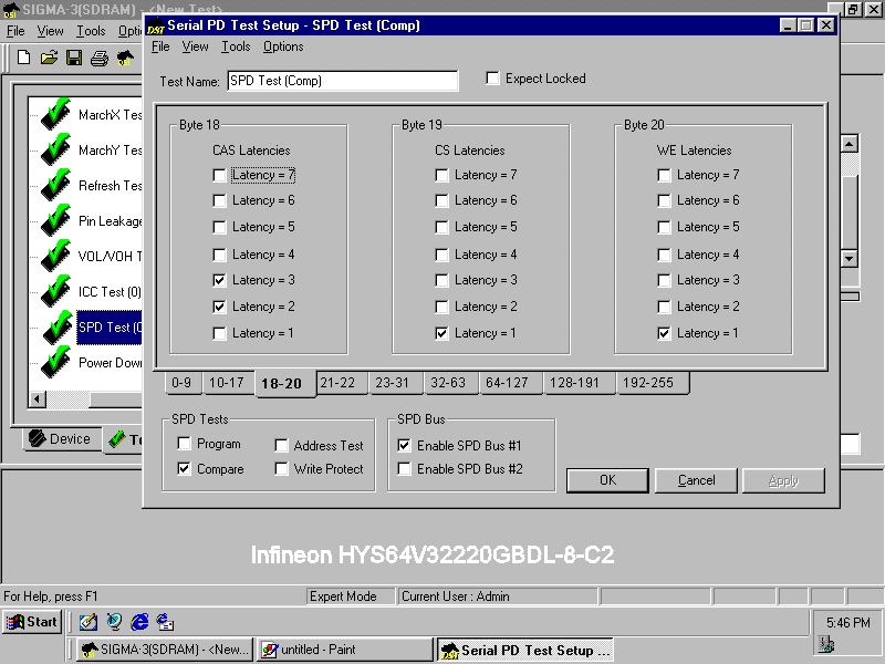 |
| The third page of SPD information shows the CAS Latency (CL) settings that the module supports in Byte 18. A quick
explanation of what this means: CL is the number of memory system clock cycles which need to occur between the request
to read a piece of data, until it is actually available. Because of the inherent delay that the memory needs to
be able to get to a particular location and provide the data there, the system needs to wait a few cycles. In this case
the amount of time this represents is the Cycle Time parameter in Byte 9, times the number of latency cycles, or 10ns
(nanoseconds) times the CL value. Therefore, for a CL2 module, at least 20ns is needed in order to guarantee that the data
is properly read. You may notice that Byte 18 shows TWO latencies are enabled; CL2 and CL3. All this means is that the module
is telling the system that either one of those CL settings is supported. |
 |
 |
| The remaining SPD pages are not important for this discussion of low vs. high density or CAS latency issues. They
contain optional areas to store the module manufacturer name, part number, serial number, etc. |
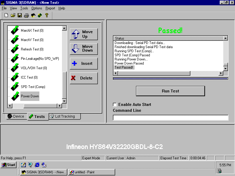 |
| Here you see the results of the test program for the Infineon module. You can't see all of the tests in the left
side window (MarchX, MarchY, Refresh, etc.) but there are several others before those listed. |
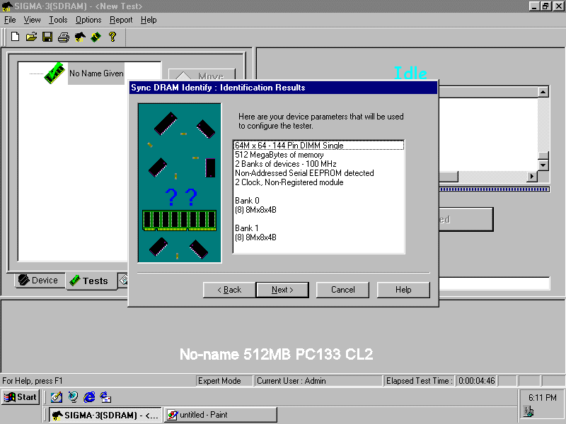 |
| As an example, I took out one of the 512MB PC133 modules in my T23 and ran the same ID wizard on that module. You can
see that it was detected as a 512MB module, two banks (sides) of memory, but only PC100. That speed is a result of an
old tester that's been out of calibration for several years :) . It still does recognize that the memory consists of
two banks of eight parts of "8Mx8x4B", or 32M x 8, double the Infineon 256MB module. And something that I can visually
confirm; the module does indeed have 16 total memory chips. |
 |
| The first page of SPD info for my 512MB module shows 13 row addresses (vs. 12 for the 256MB module) and a Cycle time
value of 7.0ns. Adding one more row addresses means a doubling of the amount of data storage, so that makes sense. It
also means that there are twice as many rows to refresh. The Cycle Time value of 7ns equates to 142.85Mhz, slightly
above the normal spec of 133Mhz (7.5ns). This is the way that a PC133 CL2 module is categorized. |
 |
| On this second page of SPD info for the 512MB module, one thing is important: the Refresh Rate. Compare this value (7.8µs)
to the one for the 256MB module (15.6µs) and you will see the difference between low density and high density memory.
The value of 7.8µs means that there must be a refresh pulse this often for proper memory refresh to occur. 7.8 is one-half
of 15.6 so this means that for the same 64ms period, TWICE as many refresh cycles are needed. In other words, this 512MB
module requires 8,192 refresh cycles to the 256MB module's 4,096 cycles. That's the difference between "high" and "low"
density memory. |
Conclusion
From the results of the Darkhorse testing I would have to say that there's a bug in that tester if the Infineon datasheet is
valid. It indicates that each memory is 8 bits wide which goes against the Infineon datasheet. It does report the SPD data
as being low density (4K refresh) which is backed up by the module working in a 600E system. The bottom line: If you are
looking for a 256MB PC100 low density part, this one will work.
Addendum (Oct. 16, 2007)
After looking at BiilP's Infineon module I started keeping my eye out on eBay for an identical module so I could perform some
surgery on it. About two weeks later, this one (link to a 138KB Adobe .PDF file) showed
up as a Buy-It-Now for $30. That's more than what I would normally pay for a 256MB PC100 module, but hey, this is a science
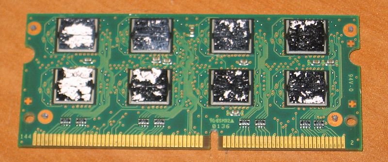
experiment :) !. The module arrived in a week and I immediately took one of the shields off and exposed this:
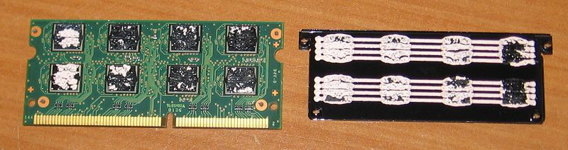 |
| The shield is held in place on the four corners with a plastic stub which has been melted down and spread out. Using
an X-ACTO knife, I simply cut the "heads" off of each and lifted the shield up. There's 8 FBGA (fine-pitch, ball-grid array)
packages on each side. The part number on the top says "HYB39S128" which I believe to be a 128Mbit SDRAM. Each part is then
16Mbyte, so a total of 16 parts makes up the 256Mbyte module. |
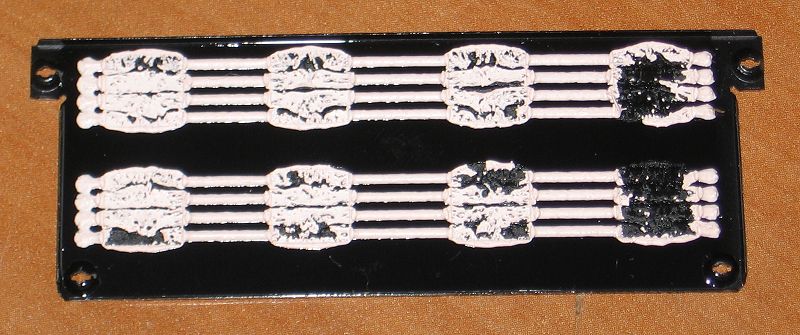
Here's a couple of close-up pictures:
Raymond Kawakami
San Jose, CA
E-Mail: r k a w a k a m i AT a o l DOT COM