October 12, 2008
 |
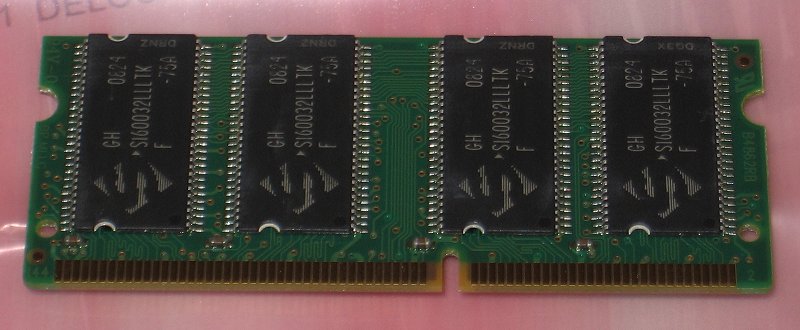 |
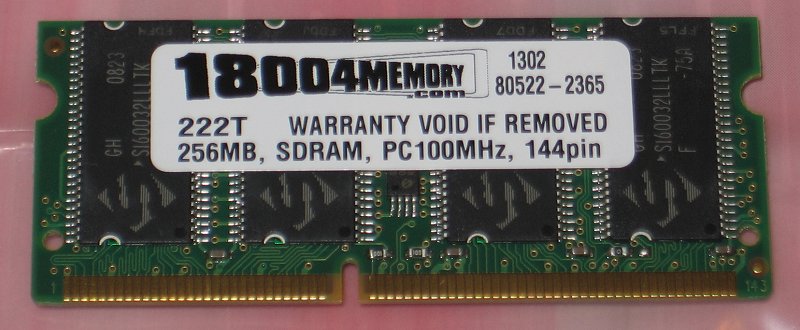
| This is the front and back views of the module I received from eBay seller "1-800-4-memory". It was advertised as being a direct replacement for IBM FRU 33L3069/33L3070 and as such, means that it should be a 256MB "low density" module. The strange thing is that there's only 8 memory components on the module. The general rule has been that if you need a 256MB low density version, you have to use the ones with 16 parts on it. | |
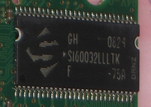 |
| This is a close-up of one of the parts on this module. The manufactuer's logo identifies this as being from SpecTek, a Micron-owned company. I've searched around their web site and have not been able to find a datasheet which matches that part number. Some of the problem is that they have changed their part numbering system at least twice in the past 4 years. |
 |
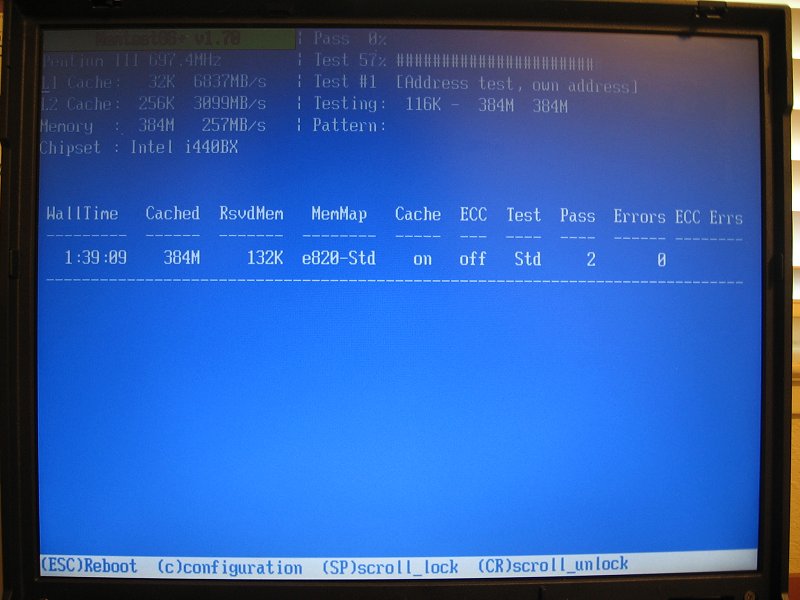 |
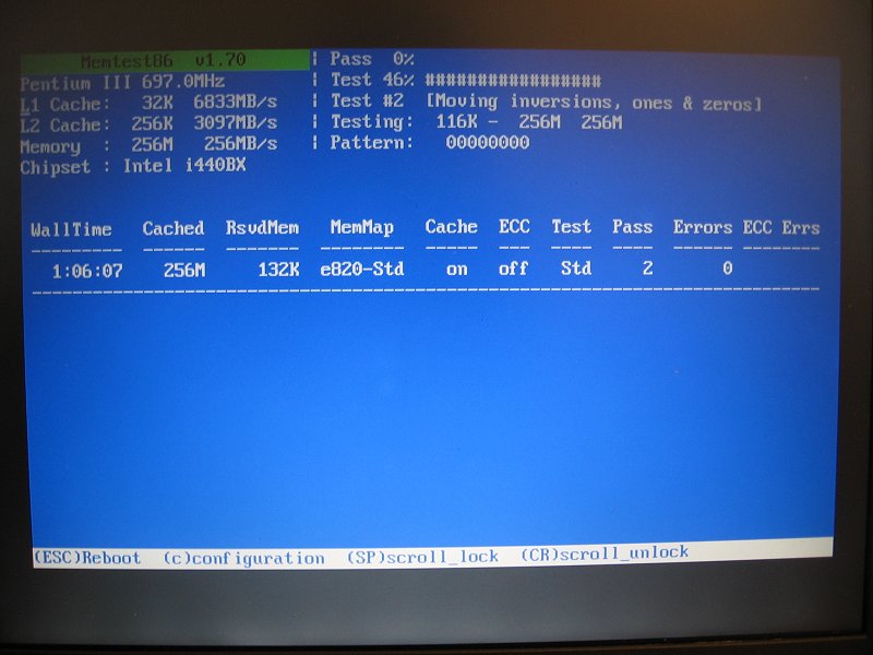
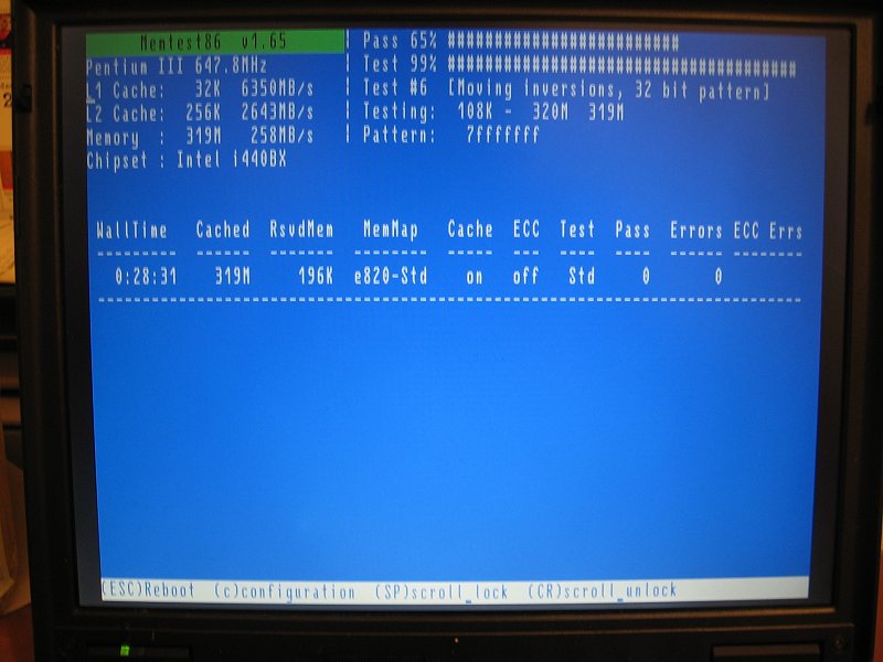
| The screen shot on the left is from the module running by itself in a T21. I ran memtest86+ for two complete passes and there were no errors. I then installed this new 256MB module in an A22p, with a low density 128MB stick. That's the photo on the right. I also tried installing a Micron 16-chip 256MB module along with this 8-chip version and memtest86+ saw all 512MB and passed all tests. | |
 |
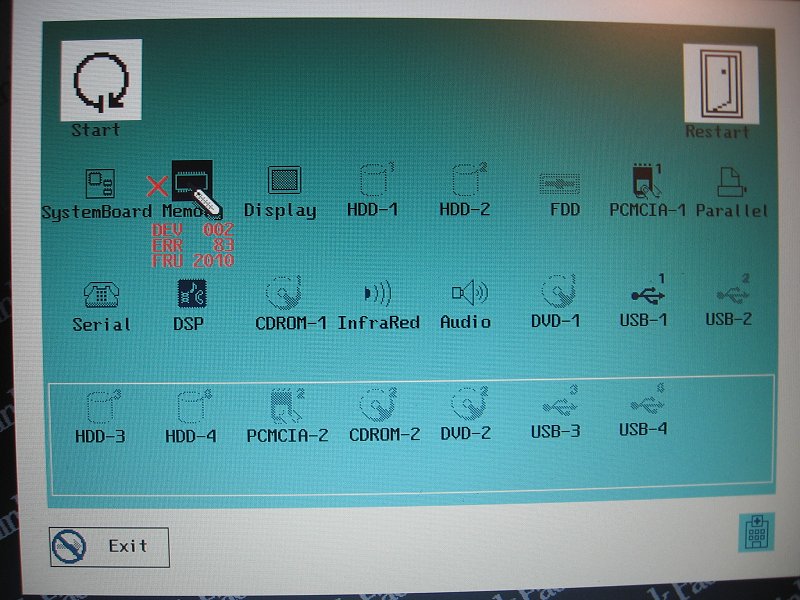 |
| Next "low density" system I tried was a 600E (2645-8AU). The picture on the left shows 288MB of memory at POST; 256MB for the SODIMM and 32MB onboard. Since the 600E BIOS has its own memory test, I tried running that one first. It indicated a fail (DEV 002 ERR 83 FRU 2010). | |
 |
 |
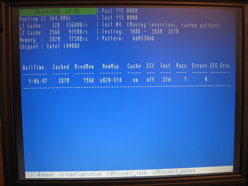
| However, running memtest86+ for an hour said everything was okay. I then put the 256MB module inside a 600x (photo on right). 320MB is indicated at POST - the 256MB module and the 64MB on the motherboard. | |
 |
|
| After about 30 minutes I took this photo, shut down the system and went to dinner. | |
I was finally able to check out this 256MB 8-chip low density module using a tester at work. What I found was pretty interesting...
 |
|
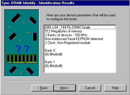
| The first screen capture above is what the tester thinks is the module. It is designed to look at an unknown (to the user) module and determine the size of the memory, but not necessarily the true top speed or the layout of the module. It says it is a 512MB module. It also thinks that there's 16 parts on the board as evidenced by the "(8) 8Mx8x4B" description for Banks 0 and 1. This appears to be an error with the tester's ID system but I was not able to confirm it with the manufacturer. | |
 |
|
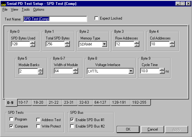
| This screen shot is some of the contents of the module's Serial Presence Detect" (SPD) information. The SPD is programmed at the factory with the module's characteristics; the type of memory, the size, speed, maufacturer ID, serial number and other data. When the memory module is installed into the computer, the computer "asks" the module, "what are you?". The SPD provides this information. If you're looking for the important data on this screen, it's the number of row and column addresses that have been programmed into the SPD. The module is telling the computer that it has 12 rows and 10 columns. That's a total of 22 address lines. For the people who know their "powers of 2" table, this represents a total of 4,194,304 (2^22) or basically, 4 Meg. Since there's a total of eight parts on this module, then that means there's essentially a total of 32 Meg (4 Meg x 8) storage locations. Because this is a 64-bit wide SODIMM, that figures out to 8 bytes per storage location (8 bits to a byte, so 64/8). Then, that's 32Meg x 8 bytes or a total of 256MB. Huh? The tester says it's a 512MB module but the SPD is saying 256MB? That's right. The module does have the ability to store 512MB worth of data, yet the module is telling the computer that it is only 256MB. This is one of the reasons how you can have a 256MB module made with only 8 memory devices. "Wait!", you're saying. "Doesn't an 8 device 256MB module also mean that it is 'high density'?" That's correct. Here's the second part to the puzzle... | |
 |
|
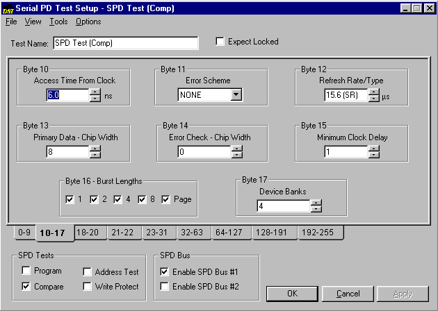
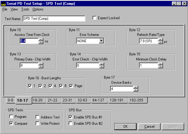
| This is the next page of data that's stored in the SPD. If you look at "Byte 12", titled "Refresh Rate/Type",
you will see a figure of "15.6 (SR)". The SPD is saying that the module requires a refresh signal every 15.6uS (microsecond). If
you have read some of my previous posts about refresh rates between "low" and "high" density SODIMMs, then you will have an idea
what this means. "Refresh" is the action required by a DRAM which enables it to retain the data that has been stored. Over time,
if nothing is done to help the memory "remember" that data, it can be lost. Modern memory design and manufacturing usually can
result in a DRAM which can retain data for a couple of seconds at room temperature. Because of the physics involved, if the memory
is subjected to an increase in temperature, the amount of time that data remains intact, decreases. Since most memory
specifications have been standardized in the industry, a period of 64mS (milliseconds) was selected as being the "worst-case"
amount of time that data can be retained without refreshing, when the device is operating at its maximum temperature. Back when
256MB SODIMMs were first offered, the state-of-the-art DRAM was based upon a 128Mbit (or 16MB) design. This also explains why you need 16 of those memories on a 256MB module (i.e., 16 x 16MB = 256MB). Those parts had a refresh specification of 4,096 (or 4K)
cycles, every 64mS. When the industry moved up to the next "density" level (256Mbit), there was a need to change the refresh spec
to 8,192 (8K; essentially because the memory size had now doubled), but keeping the overall time (64mS) the same. So the math works
out like this: "low density" DRAM requires that for every 64mS period of time, 4,096 refresh signals need to be provided. Said
another way, the computer needs to send out a refresh signal once every 15.6uS (64mS/4096). For the "high density" memory,
8,192 refreshes must be given in the same 64mS, or one every 7.8uS (64mS/8192).
Given that this 8-chip 256MB module contains "high density" memory, how can this work inside a "low density" system? This can be explained by the fact that since only one-half of the memory is being made available (by the SPD address information), it only needs one-half the number of refreshes. However, there is a danger here for at least one specifc reason that I can think of. Refreshing can be performed in several different ways. The two basic methods are to access the memory in a sequence of row addresses or to use a special timing condition called CBR (CAS-before-RAS) refresh. The first method requires that the computer's chipset is able to send out a command to access row 0, then row 1, row 2, row 3... and so on unitl it gets to row 4,095 (or 8,191) and then it resets back to row 0 for the next series of refreshes. This also means that the address sequencing is being controlled externally to the memory. The CBR refresh method does not require any such external address control since there is an address generator built into the memory itself. All the memory needs to "see" is a special timing condition on two control pins (RAS and CAS) and the memory internally generates the proper signals to refresh the data. So, what's the danger? If the memory is being refreshed using the CBR method, it is in violation of the operational specifications. Instead of all of the data being refreshed every 64mS, it will be done at a 128mS rate. There is a tiny possibility that a marginal device which passed the "normal" datasheet spec of 64mS, could fail at 128mS. As a test engineer it bugs me that this could happen but realistically, the chances of it occurring is fairly small. You would have to be operating the module at the highest temperature allowed, usually around 70c, for it to be of any concern. |
|
 |
|
| Just for grins, I also grabbed some screen captures for a 16-chip 256MB module and an 8-chip 512MB module. This is the first SPD page for the 16-chip 256MB module. The row and column addresses are set to 12 and 10; the same as the 8-chip 256MB module but we now know it's lying. | |
 |
|
| Here is the second SPD page for the 16-chip module. The refresh rate is 15.6uS, signifying that this is a "low density" version. | |
 |
|
| And finally, here's an 8-chip 512MB SODIMM. Notice that the row addresses are 13. This calculates out to a proper 512MB module. A close eye will notice that the cycle time ("Byte 9") is 7.5nS meaning that it's rated for PC133 operation. | |
 |
|
| The second SPD page for the 8-chip 512MB stick. Here the refresh rate is 7.8uS, exactly what an 8K refresh part requires. | |